

1 / 5


| Category | Parameter | Diode laser | LED | LED Advantages |
|---|---|---|---|---|
| Thermal damage | Light power | Similar | Lower thermal resistance, higher efficiency of heat dissipation. | |
| Thermal power | Similar | |||
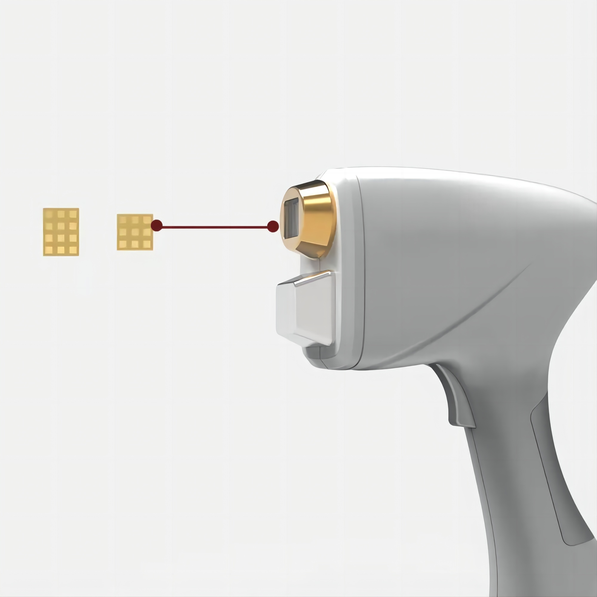
| Chip size | 1*10mm | 7.5*7.5mm | ||
| Conclusion | Similar total thermal power, LED has bigger heat dissipation are and smaller heat flow density. | |||
| Heat transfer patch | Pass to the bottom and rear Average path is 1.5mm | Pass to the bottom Average path is just 0.2mm | ||
| Conclusion | LED has very short heat transfer path, lower thermal resistance and much higher efficiency of heat dissipation. | |||
| Mechanical damage | Stress | Rectangle, high length-width ratio. Under stress of thermal deformation and thermal fatigue, chips easily desoldering or broken in pulsed working | Square, 1:1 length-width ratio. Extra thin chip and large soldering area firmly but low stress. | Lower mechanical stress. |
| Conclusion | Because of chip structure, LED chip’s stress is smaller than diode laser | |||
| Optical damage | Light power | Similar | Safer lighting surface, highly resistant to dust burning. | |
| Light emitting area | Size 0.01*0.1mm High brightness, foreign body pollution can cause light-emitting surface burned | Size 5*5mm Brightness is just similar to normal LED lamp of flashlight, slight dust will not being ignited to burn the lighting surface | ||
| Conclusion | Because of surface emitting, the brightness of LED light emitting area is much smaller than diode laser. | |||
| Chain damage | Conclusion | Not like diode laser, for LED chips, single area’s failure does not affect other emitting area | Independent emitting areas. | |

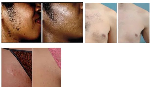
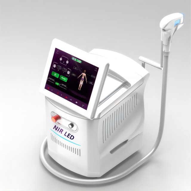
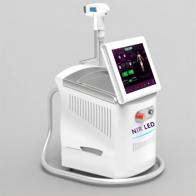
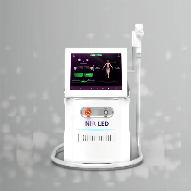
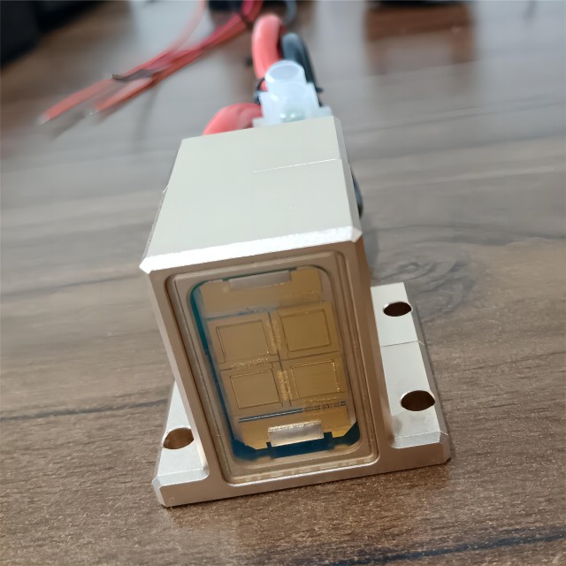
LED hair removal utilizes a high-power super-emitting LED array (containing 12 chips) as a light source. The NIR beam is shaped and transmitted through a crystal guide pyramid to target the subcutaneous tissue, allowing the melanin inside hair follicles to absorb heat and achieve effective hair removal.
While light and thermal power are similar, LED has a larger heat dissipation area and lower heat flow density. With a much shorter heat transfer path (0.2mm vs 1.5mm for diode lasers), LED offers lower thermal resistance and significantly higher heat dissipation efficiency.
The LED chip design is square with a 1:1 length-to-width ratio, featuring an extra thin chip and large soldering area for lower mechanical stress. In contrast, the rectangular shape and high length-width ratio of diode lasers can easily cause desoldering or cracking under pulsed working conditions.
LED chips have a larger light-emitting area of 5x5mm, yielding a brightness similar to a standard flashlight. This means slight dust or foreign body pollution will not ignite and burn the lighting surface. Diode lasers have a tiny 0.01x0.1mm emitting surface where high brightness makes them prone to burns from contaminants.
Unlike diode lasers, LED chips do not suffer from chain damage. A failure in a single emitting area of the LED array does not affect the performance of the remaining emitting areas, ensuring continuous functionality.