Precision-engineered hardware platforms utilizing multi-band semiconductor emitters for diverse dermatological and aesthetic phototherapy operations.


In the professional manicuring and cosmetic enhancement sectors, the transition from legacy ultraviolet CCFL (Cold Cathode Fluorescent Lamp) infrastructure to integrated solid-state semiconductor LED Nail Lamp Devices has finalized a paradigm shift. Modern polymer-based nail matrices require hyper-specific electromagnetic wavelengths to trigger rapid, cross-linked molecular polymerization without imparting thermal trauma to surrounding dermal tissues. As a top-tier manufacturer and global exporter, our operational focus centers on optimizing radiant exposure ($J/cm^2$), spectral uniformity, and diode longevity to serve high-throughput professional salons and global brand distributors.
Advanced photopolymer formulations incorporate dual-spectrum photo-initiators (primarily TPO and BAPO) that exhibit distinct absorption peaks. Traditional curing setups frequently suffered from incomplete polymer conversion, leaving volatile monomers active on the nail plate—a major cause of structural delamination and localized allergen reactions. By configuring precise dual-wavelength arrays merging 365nm (UVA1 for surface structural cross-linking) and 405nm (UVA2 for deep-layer foundational curing), our advanced electronic hardware guarantees complete, high-velocity polymerization. This systematic optimization ensures zero chemical shrinkage, high structural rigidity, and optimal safety.
Established in 2014, Shenzhen Rudiz Beauty Co., Ltd. stands as a benchmark of smart skincare technology, anti-aging beauty equipment, and advanced phototherapeutic aesthetic solutions. Nestled within the electronic manufacturing and optoelectronic innovation capital of the world—Shenzhen, China—the company has structurally scaled its operation to provide full-stack OEM and ODM capabilities for high-tier cosmetic brands, healthcare distribution entities, and international retailers.
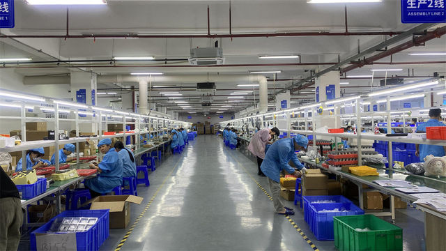
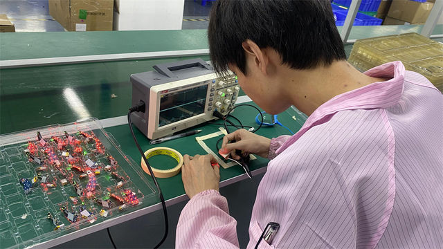
Our manufacturing topology spans an expansive 10,000 square meter modern production facility, utilizing a workforce of more than 200 technically trained specialists and optoelectronic engineering specialists. By integrating localized component sourcing, advanced automated Surface Mount Technology (SMT) suites, multi-axis CNC enclosure machining, and cleanroom optical capsule assembly lines, Rudiz Beauty maintains absolute control over component traceability and production quality. Every phototherapy array, microcurrent module, and fractional plasma unit undergoes systematic spectroscopic verification and dynamic multi-stage load simulation prior to shipping out.
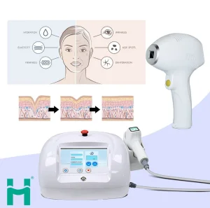
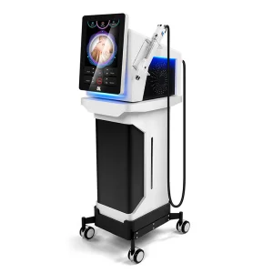
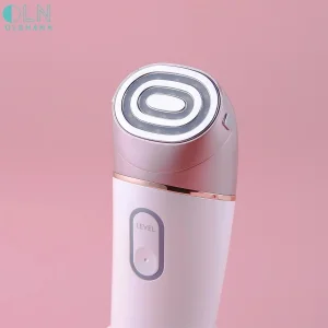
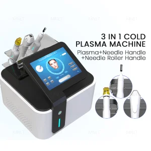
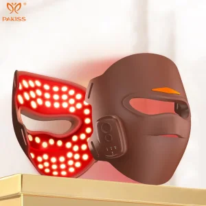
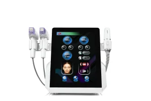
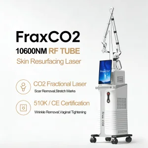
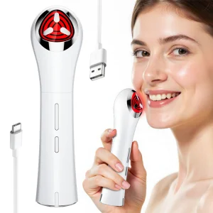
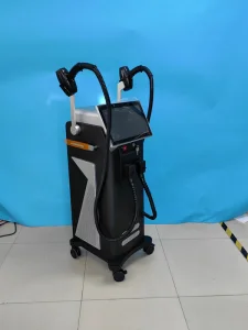
Our diversified production portfolio encompasses professional facial care apparatus, multi-handle Fractional Plasma systems, advanced Radio Frequency (RF) tissue-sculpting matrices, and smart therapeutic LED configurations. The depth of our product lines is illustrated by our specialized aesthetic systems, designed to handle both medical-grade clinic deployments and targeted, high-performance ergonomic home applications.
Enterprise-level B2B procurement demands strict compliance with international cross-border safety frameworks. Standard consumer electronics often lack the precise electrical insulation and electromagnetic shielding required for medical spas and commercial environments. Industrial-grade beauty equipment must integrate multi-tier safety architecture, including isolated galvanic step-down power electronics, over-current fault detection, and flame-retardant high-impact polycarbonate enclosures.
Our manufacturing lines operate under comprehensive international certification protocols, including CE (EMC/LVD), RoHS, FCC, and alignment with FDA performance requirements for light-emitting medical devices. We provide global supply chains with end-to-end component traceability, customized private-label injection molds, custom packaging options, and flexible, scalable production schedules designed to minimize lead times across major distribution pipelines in North America, Western Europe, and the Asia-Pacific region.
Full layout circuit design, bespoke internal chip configuration, firmware control tuning, and rapid prototype casing design.
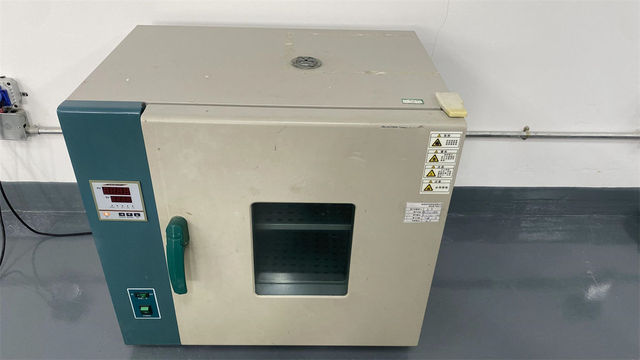
Every unit undergoes continuous full-spectrum radiometer cross-checking and 24-hour thermal stress testing before final packaging.
Optimized packaging formats designed to lower volume weight metrics, combined with integrated customs documentation processing for hassle-free entry.
The primary engineering challenge in high-intensity photo-curing devices is mitigating localized thermal spikes. When multiple high-radiance semiconductor dies operate within small physical spaces, junction temperatures can rise quickly. Unchecked heat not only decreases internal emitter conversion efficiency, but can also cause "heat spikes" that induce severe client discomfort. Our engineering team addresses this by utilizing heavy-gauge aluminum structural plates integrated with passive micro-finned heat sinks. This design keeps diode junction temperatures well below critical limits, even during intensive back-to-back salon shifts.
Additionally, our newer platforms feature integrated smart infrared distance sensors coupled with smart microprocessor control loops. When a user introduces a hand into the chamber, the device dynamically ramps radiant emittance through pulse-width modulation (PWM) instead of delivering a harsh thermal spike. This progressive curing timeline prevents excessive exothermic reactions from modern soft-gel formulations, safeguarding sensitive subungual tissues while ensuring a rock-solid polymer finish.
Integrated Therapeutic Photobiomodulation (PBM)
By blending targeted 660nm deep red-light emitters directly into our commercial curing modules, our custom solutions stimulate local microcirculation and cell repair. This minimizes skin dehydration and prevents the hyperpigmentation often linked to standard UV exposure.
The global aesthetic landscape requires specialized product features across different market segments. Our product configurations are engineered to meet these unique localized demands:
Requires heavy-duty structures with scratch-proof acetone-resistant surfaces, magnetic removable base plates for easy cleaning, and wide apertures to handle both manicures and pedicures smoothly.
Demands sleek, cohesive brand styling with high visual impact, customizable LCD timers, custom brand logo placement, and consistent color matching to elevate retail visibility.
Focuses on lightweight portability, incorporating high-capacity integrated lithium-ion battery configurations, secure USB-C Power Delivery ports, and compact, drop-resistant housings.
Looking toward the 2025–2030 horizon, the smart hardware sector is moving toward deeper ecosystem integration and increased ecological sustainability. Regulatory update trends point toward stricter controls on raw polymer toxicity and plastic circularity. Consequently, our R&D roadmap focuses on incorporating eco-friendly, PCR-recycled structural plastics without compromising structural resistance to aggressive chemical solvents like acetone.
Simultaneously, smart connectivity is entering the industrial salon landscape. Future LED arrays will leverage embedded Bluetooth and Wi-Fi modules, allowing facility managers to track real-time diode degradation metrics and optimize power settings across multiple locations via centralized dashboards. This proactive maintenance model reduces unexpected hardware downtime, helping large nail care franchises maximize operational efficiency and maintain consistent service standards.
Direct insights from our electronics laboratories and quality control managers regarding component specifications and custom B2B manufacturing options.
Our dual-wavelength configurations mount 365nm and 405nm semiconductor chips directly within the same reflective capsule. The 365nm spectral band activates surface photo-initiators to prevent surface tackiness and seal outer layers, while the 405nm band penetrates deeper gel layers to ensure complete adhesion to the nail plate, eliminating deep-layer under-curing.
We use thick, high-conductivity metal-core PCBs (MCPCBs) paired with passive structural aluminum heat dissipators to quickly transfer heat away from the electronics. Additionally, our smart firmware features a progressive low-heat mode that uses pulse-width modulation (PWM) to step up power smoothly, avoiding abrupt exothermic heat spikes.
Initial industrial design conceptualization and 3D prototyping are typically completed within 14 business days. Once the custom injection mold configurations and PCB layouts are approved, production tooling takes roughly 25 to 30 days, followed by a mass production cycle of 20 to 25 days, depending on overall order volume.
Yes, all external enclosures are molded from premium, cross-linked ABS-polycarbonate blends treated with a specialized chemical-resistant coating. This ensures the housing remains pristine and free from structural degrading, cracking, or discoloration, even with frequent exposure to pure acetone and sanitizing alcohol wipes.
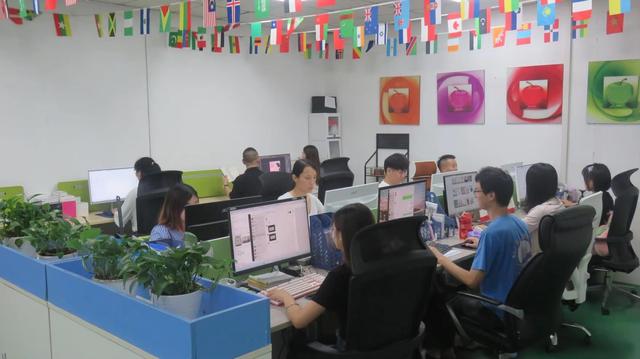
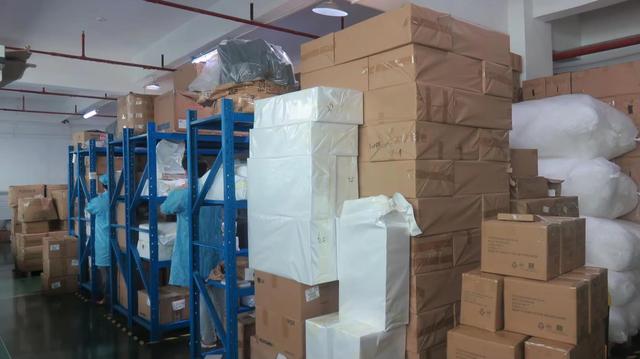
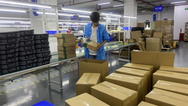
A transparent look inside our production floors, high-speed SMT assembly lines, cleanrooms, and testing facilities in Shenzhen.
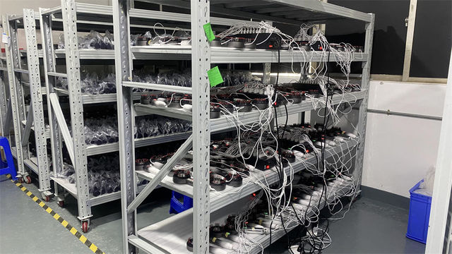
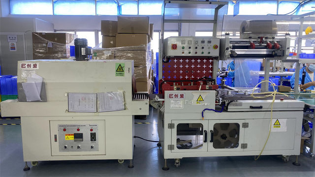
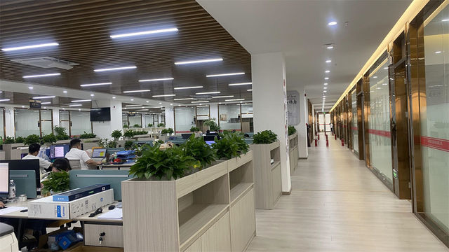
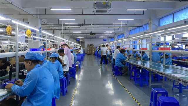
Specialized personal care hardware solutions integrating narrow-band phototherapeutic technology and precise structural thermal engineering.



 Rudiz Beauty